31688267
Semiconductor Switching Devices (Mod.3 Sect.3 Part 3) 1 of 2
Description

Slide Set by That Yeti Dog Person, updated more than 1 year ago
More
Less
|
|
Created by That Yeti Dog Person
about 3 years ago
|
|
Resource summary
Slide 1
Schematic Symbol for the Diode
Caption: : This figure illustrates the symbol for a diode. Note the position of the anode (negative) and the cathode (positive).
Slide 2
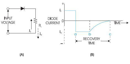
Using Diodes as Switches
Caption: : The simple diode circuit shown in Figure A produces the switching voltage and current shown by the graph in Figure B.
The abbreviation IF stands for the forward current and IR stands for the reverse current. When the input voltage is positive, the forward current (IF) flows through the load resistor. When the input voltage is negative, the diode switches the forward current off.
The graph shown in Figure B shows the switching voltage and current for the diode circuit. Note that when the input voltage is switched from positive to negative, the diode current reverses. A diode’s recovery time can be divided into two distinct parts. On the graph in Figure B, the time between a and b is called the storage time. This is the period during which the charge carriers are swept out of the P and N regions. The time between b and c on the graph is called the transition time. This is the time required for the capacitance at the diode junction to charge. The entire time between a and c (that is, storage time plus transition time) is the recovery time.
Slide 3
Step-Recovery Diode (aka Snap Diode)
If a diode’s recovery time is too slow, it makes the diode a slow switching device. Ideally, the diode current would go to zero (and stay there) as soon as the step voltage crosses the zero axis. Thus, in order to make more efficient switching devices, diode manufacturers have developed techniques to shorten diode recovery times.
In one of these manufacturing techniques, the diode crystal is doped in such a way that the charge carriers are restricted to a very narrow region around the junction of the diode. This reduces the capacitance at the junction. By altering diode construction in this way, it’s possible to make a diode with a very short recovery time. This type of diode is called a step-recovery diode, a snap diode, or a snap-off diode. (The terms snap and snap-off refer to the fact that the current snaps back to zero very rapidly.)
Caption: : The recovery time of a step-recovery or snap diode is much shorter than that of a regular junction diode.
Slide 4
Hot-Carrier Diode
Caption: : The construction of a typical hot-carrier diode is shown here.
The hot-carrier diode can also be used to reduce the recovery time in a switching circuit. In a hot-carrier diode, an N-type material is interfaced with a metal (Figure 38). When the anode is made positive with respect to the cathode, the charge carriers in the diode move rapidly and easily from the N-type material into the metal. However, when the cathode is made positive with respect to the anode, it’s virtually impossible for the charge carriers to move into the N-type material. Note that the hot-carrier diode has no depletion region, so there’s no junction capacitance to charge.
During conduction, the charge carriers that get into the anode region can’t be distinguished from the other charge carriers already present in the metal. Therefore, there are no charge carriers to be swept out of the anode region when the diode is cut off with a step voltage. The overall result is that the reverse recovery time is reduced to 50 picoseconds (50 × 10-12 seconds). The energy of the electrons entering the metal in a forward-biased hot-carrier diode is quite high. Scientists say that these electrons have a “high temperature.” Thus the term hot-carrier diode refers to the charge carriers (electrons) as they enter the metal.
Slide 5
Caption: : A simplified speed-up capacitor circuit is shown in Figure A. The graph in Figure B shows how the recovery time is reduced with a speed-up capacitor.
The Speed-Up Capacitor
Circuit designers sometimes use speed-up capacitors to reduce the transition time during diode recovery. A speed-up capacitor circuit is shown in Figure A. An input step voltage is applied to the diode circuit to charge the capacitor. When the input voltage reverses, the charged capacitor acts as a virtual short circuit (in the reverse direction) across the resistor. The charge carriers are swept rapidly out of the diode and move into the capacitor.
Notice that the reverse current (IR) and the capacitor discharge current (IC) are in opposite directions. This tends to decrease the value of IR, decrease the capacitor discharge time, and reduce recovery time.
In this circuit, the diode is actually connected in series with the capacitor. Therefore, the junction capacity and the speed-up capacity are connected in series. This reduces the overall capacity of the circuit and reduces the transition. Figure B compares the recovery time without the capacitor (dashed line) with the recovery time of the speed-up circuit.
Slide 6
Three-Layer Diode (DIAC)
Caption: : A three-layer diode is shown in Figure A and its characteristic curve is shown in Figure B.
The three-layer diode or DIAC is composed of three layers of semiconducting material, and the device has two PN junctions. A three-layer diode is actually made of two diodes connected back-to-back. Figure 40A illustrates a DIAC and Figure 40B shows the characteristic curve of the device. Three-layer diodes can be used as switching devices in electronic circuits.
When point x is made positive with respect to point y, the lower PN junction is forward-biased. However, current can’t flow immediately since the upper PN junction is reverse-biased. If the voltage across the diode continually increases, the upper PN junction will eventually reach a breakover point. When that occurs, the current rushes through the device and its resistance drops to a low value.
If point x is made negative with respect to point y, the upper PN junction is forward-biased and the lower one is reverse-biased. Again, the current can’t flow until the breakover voltage of the lower junction is reached. At that time, current again rushes through the device and the resistance becomes very low.
Since the resistance of the DIAC drops to a low value when it’s conducting, it’s important that the device never be connected into a circuit directly across a voltage source. A current-limiting resistor should always be connected in series with a DIAC.
Slide 7
Four-Layer Diodes
Caption: : The model in Figure A shows that a four-layer diode has three PN junctions. In the characteristic curve shown in Figure B, note that the diode breaks over when the anode is positive with respect to the cathode. Figure C shows two four-layer diode symbols. The symbol on the right is the more popular of the two. As with the DIAC symbols, the circles are optional.
The four-layer diode (also called a Shockley diode) is composed of four layers of semiconductor material, and the device has three PN junctions. Because of the three junctions this diode is sometimes called a PIN-PIN diode. Figure A illustrates a four-layer diode, Figure B shows the characteristic curve of the device, and Figure C shows two symbols for the diode. Note that the three PN junctions are labeled X, Y, and Z in the figure.
When a four-layer diode is forward-biased (with a positive voltage on the anode and a negative voltage on the cathode junctions), junctions X and Z are forward-biased, and junction Y is reverse-biased. For a small amount of forward voltage, the reverse bias on junction Y prevents the diode from conducting. However, as soon as the voltage on junction Y exceeds the breakover point (the zener value of junction Y ), the diode begins to conduct. A rush of current then flows through the device.
When the diode is reverse-biased, junctions X and Z are reverse-biased and junction Y is forward-biased. Four-layer diodes can’t operate in the zener region, so the reverse voltage must not be able to reach the zener point shown on the characteristic curve in Figure B.
Slide 8
Tunnel Diodes
Caption: : The characteristic curve for a tunnel diode is shown in Figure A. The symbol for the device is shown in Figure B.
Figure A shows the characteristic curve for a tunnel diode, and Figure B shows the symbol used to represent tunnel diodes. On the characteristic curve, note that when the applied voltage is negative (-V), the reverse current (-I) increases rapidly. When the forward voltage is increased from 0 to VA, the diode current increases rapidly to point b on the curve. A further increase in voltage causes a decrease in current from point b to point c. Beyond point d, the conduction increases as in a typical rectifier diode.
Tunnel diodes aren’t used in new designs, but they’re still available for replacements in older systems.
Slide 9
Backward Diodes
Caption: : The characteristic curve for a backward diode is shown in Figure A and its symbol is shown in Figure B.
By slightly modifying the doping and junction configuration of a tunnel diode, a backward diode can be produced. A backward diode produces the characteristic curve shown in Figure A. Although normal diodes conduct when a positive voltage is applied, the opposite is the case with the backward diode. In the characteristic curve of the backward diode, note that the current starts to flow as soon as the voltage becomes negative. Because the characteristic curve of the backward diode is similar in many ways to that of a tunnel diode, a backward diode is sometimes called a tunnel rectifier. The symbol for the backward diode is shown in Figure B.
Slide 10
Unijunction Transistors (UJT)
Caption: : The symbol for a P-type emitter UJT is shown in Figure A. Figure B shows the construction of a UJT ohmic or ordinary contact base connection. These connections allow current to flow in either direction. The equivalent circuit in Figure C shows UJT operation and Figure D shows the UJT characteristic curve.
The ohmic or ordinary contacts are base connections at each end of the device. These contacts are called Base 1 and Base 2 and are labeled B1 and B2 in Figure B. These contacts aren’t rectifying connections; they allow current flow in both directions. Thus, the contacts are called “ohmic.”
The single rectifying connection in the UJT is the PN junction from the emitter. The resistance of the base section between B1 and B2 is called the base-to-base or interbase resistance, and is usually labeled RBB. The value of interbase resistance varies from about 5 kΩ to 10 kΩ Internally, the base resistance acts like a voltage divider, dropping the bias voltage (VB) along the length of the resistance.
Slide 11
Programmable Unijunction Transistor (PUT)
It’s sometimes desirable for the circuit designer to determine the breakover point of a device. Electronics manufacturers supply a special unijunction transistor called a programmable unijunction transistor (PUT ). The word “programmable” simply means that the designer can set the voltage at which the device breaks over. This feature gives the designer better control over the circuitry.
The RC network (R1C) is used to set the frequency of the device. The voltage across the capacitor must reach a certain value before the PUT conducts. That value is obtained by setting a specific voltage on the gate.
The gate voltage is determined by a voltage divider consisting of RA and RB. When the voltage at the junction of R1 and C exceeds this voltage, the UJT will conduct and produce a very fast discharge current through the capacitor (C). During this discharge time, the voltage across resistor R2 has a short duration positive value.
The frequency of the output pulses (and of the sawtooth) can be changed by simply changing the ratio of RA to RB in the voltage divider. Usually, RA is made the variable when the frequency is to be varied.
Caption: : The symbol for a programmable UJT is shown in Figure A. In the PUT oscillator circuit shown in Figure B, the solid arrows show the charge path for the capacitor (C) and the broken line shows the discharge path.
Slide 12
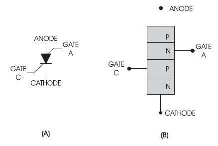
Silicon-Controlled Rectifier (SCR)
Caption: : The SCR symbol is often used in schematics without the enclosing circle as shown in Figure A. The construction model for an SCR is shown in Figure B. Both reverse and forward breakover points are indicated on the SCR characteristic curve shown in Figure C. In practice, the reverse breakover voltage is designed to be at least equal to the forward breakover voltage.
You can think of an SCR as an NPN transistor with an extra P-type layer. To operate the SCR, the anode is normally made positive with respect to the cathode. However, the device can’t conduct without a gate voltage because the center PN junction is reverse-biased.
If a positive voltage is applied to the gate, a large number of charge carriers are drawn across the lower junction, and the device begins to conduct. (Note that the NPN junctions in the lower part of the model act very much like an NPN transistor.) If a reverse voltage is placed across the SCR, it won’t conduct, since it’s a type of diode.
Figure C shows the characteristic curve for an SCR. The positive voltage on this curve is applied between the anode and the cathode and the current is through the device. The point where the forward breakover voltage occurs is set by the positive voltage on the gate.
If there’s a positive voltage on the anode of an SCR (with respect to the cathode) it’s ready for conduction. It won’t conduct, however, until a positive current pulse is applied to the gate. Once the SCR goes into conduction, the gate has no further control.
It’s a common misconception that the SCR is started into conduction by a voltage pulse. However, that isn’t the case. A current pulse is required. Typically, conduction is stopped by taking the positive voltage away from the anode.
Slide 13
SCRs in a Circuit - Static Switch
A basic circuit that illustrates the operation of an SCR is shown in this figure. This circuit is referred to as a static switch. In the circuit, the SCR is connected in series with a lamp. When switch S1 is closed as shown in Figure A, no current flows through the device (the gate is open) but there’s a voltage across the SCR.
In Figure B, switch S2 is closed momentarily. This puts a positive pulse on the gate and causes the SCR to begin conducting. When S2 is released as shown in Figure C, there’s no longer a positive gate voltage. However, the SCR continues to conduct and the lamp remains on. The only way to turn this lamp off is to open switch S1 and break the circuit path. If S1 is opened and then closed again, the lamp will go off. It will remain off until S2 applies a positive trigger to the gate again.
Why is the circuit constructed this way? Why not just connect a switch in series with the lamp in order to turn the circuit on and off? The answer is that by using an SCR in the circuit, only a very small positive gate voltage will turn the SCR on. Also, once it’s turned on, a very large SCR current will flow. That means that a switch with a very low voltage and power rating can be used to control the ON/OFF condition of a high-voltage or high-current lamp.
Caption: : When S1 is closed as shown in Figure A, there’s no current through the SCR and the lamp is off. When S2 is momentarily closed as shown in Figure B, the gate of the SCR is made positive and the lamp is turned on. However, when S2 is opened as shown in Figure C, the lamp remains on because the gate no longer has control over the anode current.
Slide 14
SCRs in a Circuit - AC Static Switch
Caption: : In an AC static switching circuit, the lamp remains off when switch S1 is closed, as shown in Figure A. In Figure B, current flows through the SCR when S2 is closed to turn the lamp on. However, upon opening S2, the SCR immediately stops conducting and the lamp goes off as shown in Figure C. In Figure B, note the one-half waveform of the current produced when an SCR is used in an AC circuit.
As long as S2 remains closed, the lamp remains on. However, when S2 is opened, the lamp goes off (Figure C). The reason for this is that the applied AC voltage goes from zero to its peak value, then back to zero again. As soon as the AC voltage on its anode goes back to zero, the SCR turns off, turning off the lamp. Thus, this figure shows that an SCR can be turned off by dropping its anode voltage to zero.
Note that an SCR causes half-wave current rectification in an AC circuit. This can be a disadvantage or an asset in a circuit, depending on the application.
Slide 15
The TRIAC
Caption: : A TRIAC symbol is shown in Figure A. Note the similarity of the TRIAC symbol to the DIAC symbol. A model of a TRIAC is shown in Figure B. You can see from the model why a TRIAC behaves like two SCRs connected in inverse parallel.
In the previous section, you saw how the SCR causes half-wave current rectification. This prevents the lamp circuit from achieving full brightness. To get around this problem, a triode AC semiconductor switch (TRIAC) can be used in the circuit. A TRIAC, or a bidirectional thyristor, can conduct in both directions, so it behaves like two SCRs connected back-to-back or in inverse parallel.
The TRIAC operates much like an SCR in a circuit, except that the TRIAC will cause a full-wave current to flow through the load and the device.
Keep in mind that the SCR and TRIAC are both very fast switches. That means they can be turned on or turned off almost instantly. In fact, they can be turned on and off in such a way as to limit the current through the load to some portion of a half-wave or full-wave AC signal.
Slide 16
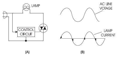
The TRIAC 2
Caption: : The operation of a TRIAC is shown in Figure A. The control circuit determines when the TRIAC turns on and allows current to flow through the lamp. The waveform in Figure B represents the lamp current.
The TRIAC gate is operated by a control circuit that’s used to deliver a positive gate pulse. This gate pulse arrives some time after the input AC power has gone through its 0 V value.
The waveform in Figure B shows that the AC current doesn’t start to flow through the lamp until an instant of time after the applied AC voltage has passed 0 V. The overall result is that the lamp won’t glow as bright because the current isn’t on as long as it would be without the TRIAC circuit. The control circuit can be adjusted so that the pulse arrives sooner (for more brightness) or later (for less brightness).
Slide 17
The Silicon-Controlled Switch (SCS)
Caption: : The symbol for an SCS is shown in Figure A. You can see from the symbol that the SCS is an SCR with two gates. In the SCS model shown in Figure B, the only difference from the SCR model is the addition of Gate A.
A silicon-controlled switch (SCS) can be thought of as an SCR that has two gates. Gate A (which stands for the anode gate) is connected to the N region of a PNP device. Therefore, a positive pulse on the SCS is useless. A negative pulse is required to turn that PNP section on. Gate C (which stands for the cathode gate) is the ordinary gate of an SCR. It turns the device on with a positive-going pulse. The SCS symbol is shown in Figure A and the SCS model is shown in Figure B.
There are two advantages in having the extra gate. The first advantage is that the SCS device can turn on with either a positive or a negative gate pulse, while the SCR requires a positive gate. As a result, a circuit designer is allowed more flexibility when using the SCS. The second advantage is that Gate A can be adjusted with a slight positive voltage to make the SCS less sensitive to turn-on, and therefore resistant to noise impulses. Gate A can also be operated with a slight negative pulse so that less current is required to turn on Gate C.
The silicon-controlled switch can be operated as an SCR by leaving Gate A unconnected. The SCS is unusual in this regard because most electronic devices may never be operated with an open electrode.
Slide 18
Silicon Unilateral Switch (SUS) & Silicon Bilateral Switch (SBS)
Caption: : The symbol for an SUS is shown in Figure A. The symbol for an SBS is shown in Figure B.
Two other switching devices of interest are the silicon unilateral switch (SUS) and the silicon bilateral switch (SBS). An SUS can be thought of as a miniature SCR, but it’s really more closely related to the unijunction transistor. The only difference between an SUS and a UJT is that the turn-on voltage of the SUS is a fixed value, while the voltage value of the UJT is dependent on the intrinsic standoff ratio. In addition to its use in switching circuits, the SUS is used in counters and oscillators, and as an SCR trigger.
The SBS behaves very much like two SCRs connected back-to-back. Once the SBS is turned on, it has a characteristic operation that’s almost identical to the TRIAC. Recall that the TRIAC can conduct in both directions, while the SCR can conduct only in one direction. Thus, the SBS is much like a miniature TRIAC. The SBS is used both in switching circuits and counters, and as a TRIAC phase control.
Want to create your own Slides for free with GoConqr? Learn more.